CAD adjustment for simulation purposes
Simplifying a CAD file involves reducing the complexity of CAD models while preserving essential design features and functionalities, with a particular emphasis on improving the efficiency of simulations. In CENOS Radio Frequency, simplifying CAD files can significantly speed up the simulation process.
We have summarized the main aspects for a simulation-friendly CAD file, which should be followed to create simple, trouble-free geometry for your simulation. This procedure includes various techniques to make the models more manageable for simulation purposes. This involves reducing the number of components and removing unnecessary details that do not contribute to the simulation objectives. In this way, it is possible to minimize computing resources and reduce the time required for simulations and analysis.
Unnecessary elements
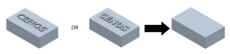
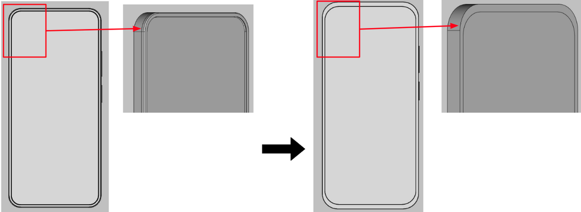
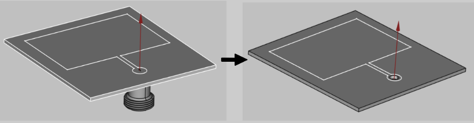
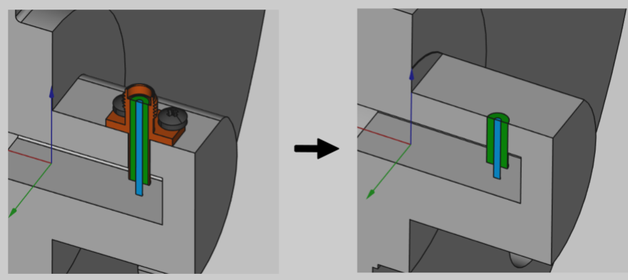
Unnecessary elements in a CAD model are features that do not contribute to the simulation’s objectives and can be safely removed without affecting the accuracy of the results. These elements can include fine details that are irrelevant to the simulation context. Parts, such as embedded text can be taken out of your model.
Small holes and fillets might be critical in a physical product for assembly or stress distribution but are often redundant in a simulation aimed at analyzing electromagnetic characteristics.
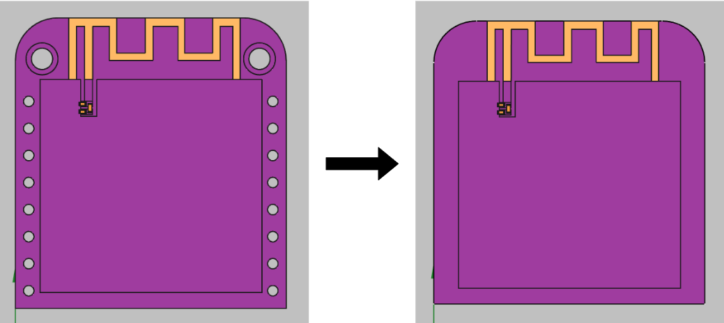
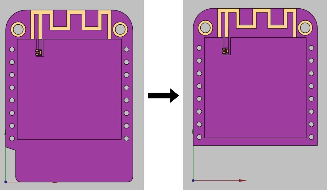
In PCB models, it is common to include silkscreen layers that provide visual and textual information that helps in the assembly and maintenance of electronic components. However, these elements are not relevant in the simulation process and can be removed, thereby allowing for the generation of a less complex mesh.
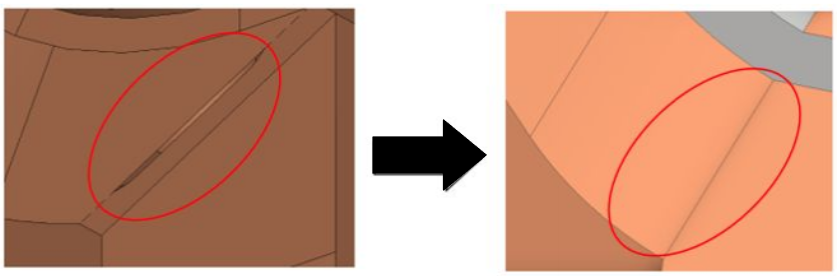
If you consider that any of these elements are necessary in the simulation, try to simplify it as much as possible. For example, you can replace the curvatures and threads of a bolt with simple cylinders.
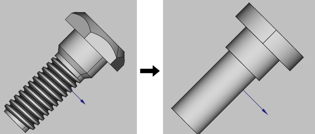
Pay close attention to surfaces with curvatures, as these significantly increase the number of elements in the mesh. The increased element count can lead to longer simulation times and higher computational resource requirements. Therefore, try to reduce as many curvatures as possible.
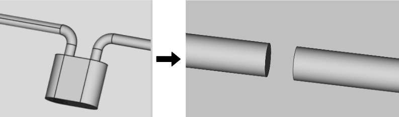
Port simplification
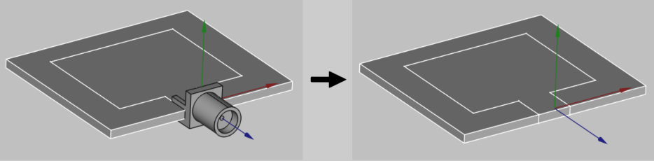
The port or feed is one of the most important parts of the assembly, however, you can easily simplify the port geometry, to make the simulation faster without significant losses in accuracy.
Gaps & Overlapping
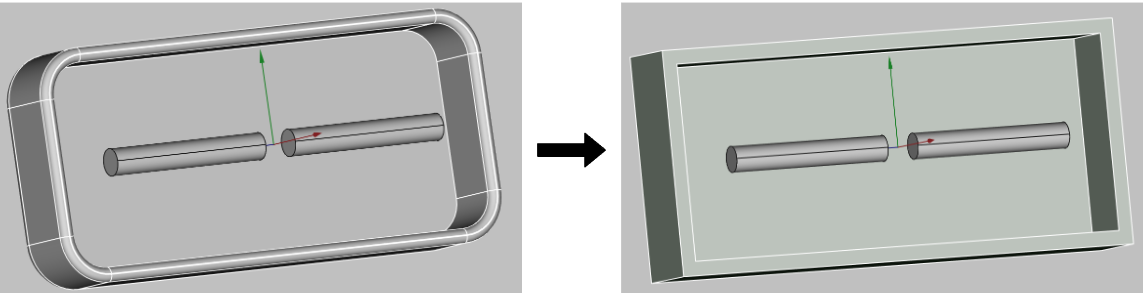
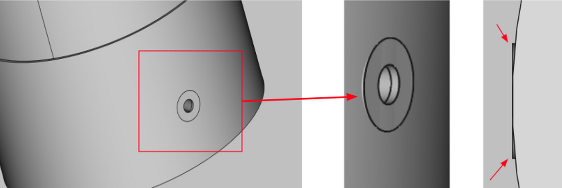
It is crucial that your geometry remains continuous. Please ensure there are no overlappings or gaps, as these can lead to meshing problems and calculation errors. Maintaining accuracy in your connections is essential for reliable simulations and precise results.
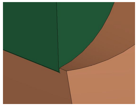
Sometimes, gaps that go undetected by the naked eye can cause issues with the meshing of your geometry. We recommend zooming in on the joints of your model to ensure that no components overlap or leave small gaps between them. Maintaining close inspection at these critical points will help prevent potential meshing problems.
PCB simplification
Model minimization
Minimizing your CAD model is essential to enhance the performance and efficiency of RF simulations. By reducing the complexity of your model while retaining the necessary details, you can significantly improve the simulation process.
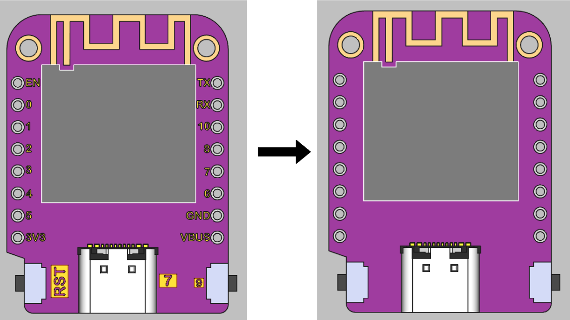
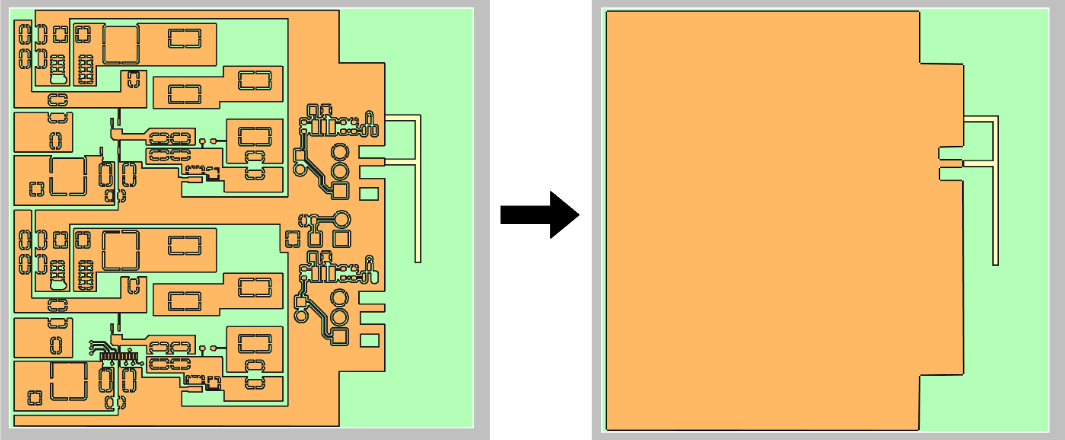
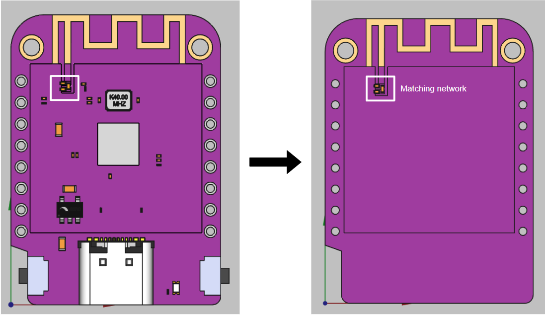
In many cases, the PCB to be simulated is used for different purposes or contains elements whose functions do not affect the primary element being simulated. In such cases, it is possible to reduce the model to include only the relevant elements.
Simplification of conductive layers
One effective way to simplify conductive layers is to reduce the detailed geometry of conductive traces and elements. This involves replacing minute details with simpler representations that retain the essential electromagnetic characteristics. For example, very thin traces or complex patterns can be represented by wider traces or simplified patterns that capture the core functionality without the excess detail that could complicate the simulation.
In some cases certain details of the conductive layers may be irrelevant to RF analysis. Identifying and eliminating these details can significantly reduce the complexity of the model. Grouping conductive components within regions of the interest can simplify the simulation. Instead of addressing each element individually, nearby or functionally related components can be grouped into a single representative entity.
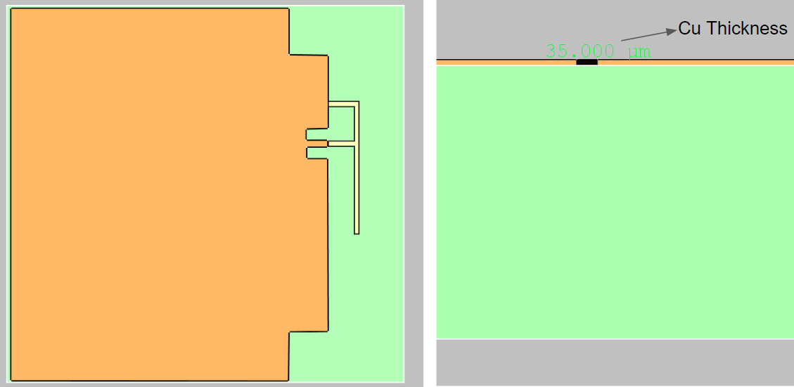
When the conductive layers are of a substantially small thickness (≤50 µm), they can be approximated as 2D surfaces rather than using the 3D layer.
Component reduction
In RF simulations, not all components on a PCB contribute equally to the behavior of the radio frequency signals. Passive components may have minimal impact on the antenna or RF part simulated. Because of this, they can often be simplified or omitted. Similarly, decorative or non-functional components, like mounting holes or mechanical supports, should be considered for removal if they do not influence the electrical performance.
Passive components simplification
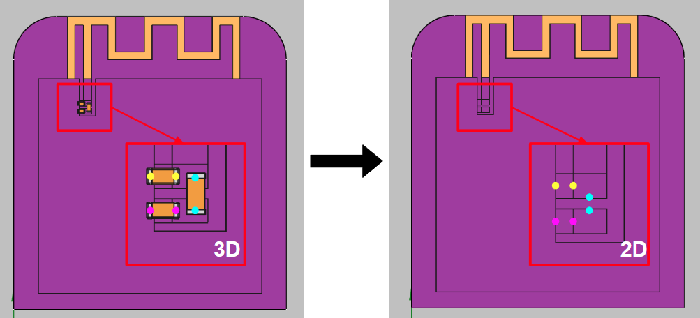
The role of passive components, such as resistors, capacitors, and inductors, is fundamental in RF circuit design. However, the 3D components can significantly increase the complexity of CAD models. In CENOS RF, such components can be simulated using lumped elements, which are assigned in the Geometry section. Therefore, in your CAD model, these components can be simplified as simple 2D patches.
In the following image you will see what passive components would look like without including 3D elements. Each colored dot represents one of the terminals of the lumped elements to be used to make a correct representation of these elements. Each terminal should be connected to the corresponding pad, just as it is done in the actual model.